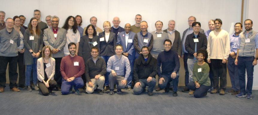
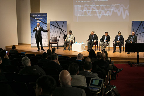
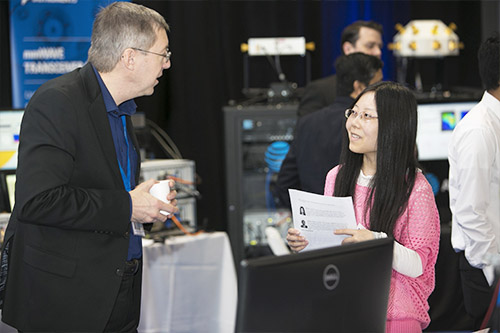
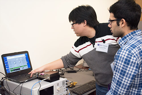
 NYU WIRELESS Workshop Convened in January
 Elza Erkip and Marwa Chafii Honored by Women in 6G
 Postdoctoral Opportunities with NYU Wireless
Our group is involved in developing novel nanotechnology solutions to the challenges facing giga- and tera-scale integration. This includes using new physical concepts, new materials, creative devices, circuits and architectures to improve system functionalities in the existing semiconductor technologies and implement completely new nano-systems for maximum benefit.
The last few decades have witnessed an unprecedented growth in the performance of the CMOS technology that now has a market share of more than $270 billion. This era also witnessed many new circuits and system concepts to support the momentum of growth in the industry. However, now electrical engineering is at its crossroads. Research in nanoelectronics must undergo a paradigm shift as the CMOS scaling approaches its ultimate limits. The next decade will usher us into an era of new science and disruptive technologies. Research involving the integration of various novel concepts – from new materials to new architectures – is necessary for enabling unique functionality beyond just high-performance general-purpose computing.
From the many research frontiers now expanding, we are specifically working in two areas: (i) terahertz wireless communication to meet the exploding bandwidth demands of the consumers and (ii) developing device and circuits concepts for computing with magnets, which offer the ultimate thermodynamic limits of computation governed by Landauer’s principle.
CURRENT RESEARCH:
- III-Nitride Transistors for Millimeter-Wave and Beyond Applications
- Low-Power Fully Digital Transceivers
- Terahertz Band Wireless Communication Via Graphene
Computing with magnets
In the last several decades, productivity of the semiconductor technology has increased by a factor of more than a billion. The rapid growth in the semiconductor industry is a direct result of dimensional scaling allowing for microprocessor chips to pack more functionality per cost. However, we are now at the 7nm node (IBM) and continued scaling would only mean more leakage, resulting in an exponential increase in power dissipation. Hence the need of the hour is a beyond CMOS technology that overcomes the hurdles imposed by scaling constraints.
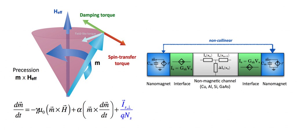
The discovery of the Giant Magnetoresistance (GMR) in 1988 paved the way for spintronics based devices like Magnetic Tunnel Junctions (MTJ) and Magnetic RAMs, and since then spintronics has become a fast emerging frontrunner in this race of beyond CMOS technologies. The use of electron spin, rather than its charge, gives spintronics devices an additional degree of freedom. Among the potential alternatives, devices based on nanoscale magnets in the field of spintronics have received special attention thanks to their advantages in terms of robustness and enhanced functionality. Magnets are non-volatile: their state remains even if the power to the circuit is switched off. Thus, the circuits do not consume power when not used – a very desirable property for modern tablets and smart phones. Virtually near-zero leakage, high integration density and high speeds have made such devices very popular.
We at the Quantum Nanoelectronics Lab at NYU are involved in analyzing the underlying physical principles of nanomagnets and their dynamics, and developing spintronics based magnetic memories and logic devices. By running Monte Carlo simulations for the magnetization dynamics of nanomagnets, we hope to understand the complex interplay between the injected spin current, the pulse duration, the probability of switching, the delay and the energy involved, among other quantities. We are attempting to build an analytical model of the switching mechanisms of nanomagnets, which will allow us to create faster low-power spin-transfer torque MRAMs.
Another facet of our research involves using Giant Spin Hall Effect (GSHE) logic devices for stochastic computing. We are currently developing compact scalable models for stochastic nanomagnet dynamics in the GSHE switch, which will allow us to create a suite of magnetic switches in a stochastic spin library (SSL) containing the timing, energy, and error probability descriptions of spintronic standard cells.
Sub-THz Materials
Our group is involved in developing novel nanotechnology solutions to the challenges facing giga- and tera-scale integration. This includes using new physical concepts, new materials, creative devices, circuits and architectures to improve system functionalities in the existing semiconductor technologies and implement completely new nano-systems for maximum benefit.
Journal Articles
| Citation | Research Areas | Date |
|---|
Conference Papers
| Citation | Research Areas | Date |
|---|